Highlights
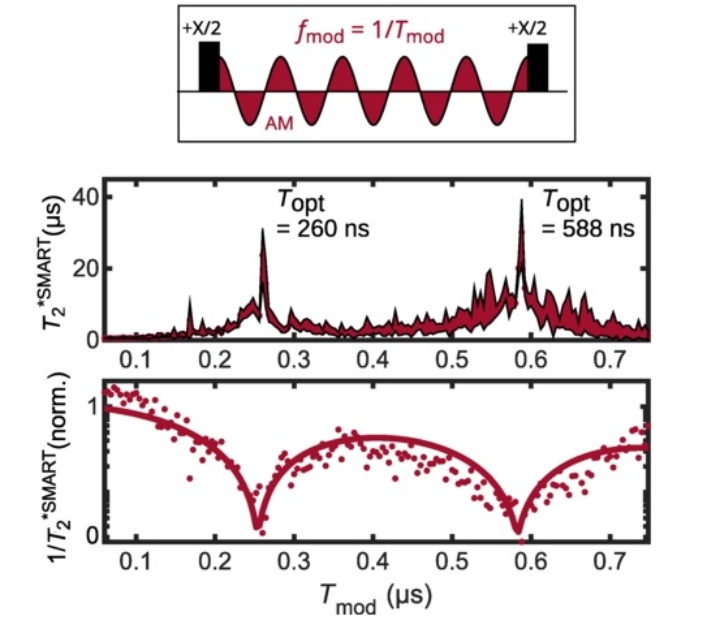
We show how the sinusoidally modulated, always rotating, and tailored (SMART) protocol, an extension of the dressed-qubit concept, can be implemented for continuous protection to offer Clifford gate fidelities compatible with fault-tolerant schemes, whilst prolonging the coherence time of a single NV− qubit at room temperature. We show an improvement in the average Clifford gate fidelity from 0.940±0.005 for the bare qubit to 0.993±0.002 for the SMART qubit, with the nitrogen nuclear spin in a random orientation. We further show a ≳30 times improvement in the qubit T∗2 coherence times compared to the bare qubit. This work paves the way for a practical implementation of a quantum computer that requires robust qubits that are protected against their noisy environment.
The state of Baden-Württemberg is building the Centre for Applied Quantum Technology (ZAQuant), an interdisciplinary research facility, at the University of Stuttgart in Vaihingen. The demands on the building when planning the layout and structural engineering were high, because the research has to take place with the least possible interference from low-frequency magnetic fields. Combar, a reinforcement element made of glass fibre composite material developed by the building component manufacturer Schöck which prevents magnetic interference caused by steel reinforcements was used here.
Applications of quantum technologies will require an unprecedented level of complexity and control of the system at the nanoscale, while retaining precision and scalability in the fabrication. The identification and characterization of suitable elementary building blocks for such technologies is crucial.
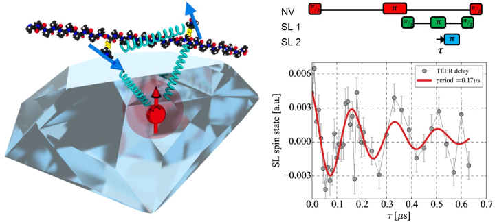
Here we present such a basic unit, a synthetic polypeptide chain with electronic spin bearing side groups. These so called spin labels are attached at specific sites of the molecular backbone using chemistry methods and separated at almost arbitrary distances, here a few nanometers. The molecular spins are controlled and read out using a nitrogen vacancy (NV) center in diamond, which provides pure optical access of single quantum states. We demonstrate the feasibility of coherent spin manipulation and access of the direct dipolar coupling tensor of pairs of S=1/2 electronic spins close to the single molecular level (≤ 3 doubly labeled molecules). The pairwise dipolar coupling of spins is found to be ~5.5 ± 1 MHz, in agreement with the designed intra-molecular spin-spin distance.
These results show for the first time, that arbitrary molecular quantum spin networks can be accessed on the single molecular level, thus opening the path to applications like molecular quantum simulators, quantum information processing, or single molecular structure determination.
Reference: Molecular quantum spin network controlled by a single qubit, Lukas Schlipf, Thomas Oeckinghaus, Kebiao Xu, Durga Bhaktavatsala Rao Dasari, Andrea Zappe, Felipe Fávaro de Oliveira, Bastian Kern, Mykhailo Azarkh, Malte Drescher, Markus Ternes, Klaus Kern, Jörg Wrachtrup, Amit Finkler, Science Advances 2017
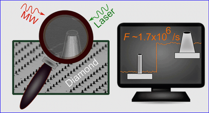
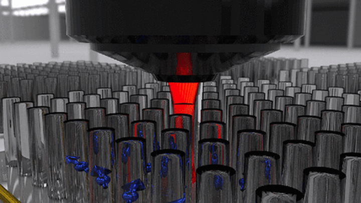
Photonic structures in diamond are key to most of its application in quantum technology. Here, we demonstrate tapered nanowaveguides structured directly onto the diamond substrate hosting shallow-implanted nitrogen vacancy (NV) centers. By optimization based on simulations and precise experimental control of the geometry of these pillar-shaped nanowaveguides, we achieve a net photon flux up to ∼1.7 × 10⁶ s–1. This presents the brightest monolithic bulk diamond structure based on single NV centers so far. We observe no impact on excited state lifetime and electronic spin dephasing time (T2) due to the nanofabrication process. Possessing such high brightness with low background in addition to preserved spin quality, this geometry can improve the current nanomagnetometry sensitivity ∼5 times. In addition, it facilitates a wide range of diamond defects-based magnetometry applications. As a demonstration, we measure the temperature dependency of T1 relaxation time of a single shallow NV center electronic spin. We observe the two-phonon Raman process to be negligible in comparison to the dominant two-phonon Orbach process.
Reference: dx.doi.org/10.1021/nl503326t | NanoLett. 2015, 15, 165-169
Author(s): S. Ali Momenzadeh, Rainer J. Stöhr, Felipe Favaro de Oliveira, Andreas Brunner, Andrej Denisenko, Sen Yang, Friedemann Reinhard, and Jörg Wrachtrup
Silicon carbide is a promising platform for single photon sources [1], quantum bits (qubits), and nanoscale sensors [2] based on individual color centers. Toward this goal, we develop a scalable array of nanopillars incorporating single silicon vacancy centers in 4H-SiC, readily available for efficient interfacing with free-space objective and lensed-fibers.
A commercially obtained substrate is irradiated with 2 MeV electron beams to create vacancies. Subsequent lithographic process forms 800 nm tall nanopillars with 400–1400 nm diameters. We obtain high collection efficiency of up to 22 kcounts/s optical saturation rates from a single silicon vacancy center while preserving the single photon emission and the optically induced electron-spin polarization properties. Our study demonstrates silicon carbide as a readily available platform for scalable quantum photonics architecture relying on single photon sources and qubits. The joint work of the international team of researchers in the US, Germany, Korea, Sweden and Japan have published the work in Nano Letters [3].
References
[1] M. Widmann, S.-Y. Lee, T. Rendler, et al., Coherent control of single spins in silicon carbide at ambient condition , Nat. Mater. (2015) 1–21.
[2] M. Niethammer, M. Widmann, S.-Y. Lee, P. Stenberg, O. Kordina, T. Ohshima, et al., Vector Magnetometry Using Silicon Vacancies in 4H-SiC Under Ambient Conditions, Phys. Rev. Appl. 6 (2016)
[3] M. Radulaski & M. Widmann, M. Niethammer, J.L. Zhang, S.-Y. Lee, T.
Rendler, et al., Scalable Quantum Photonics with Single Color Centers in Silicon Carbide, Nano Lett. 17 (2017) 2–6.


